
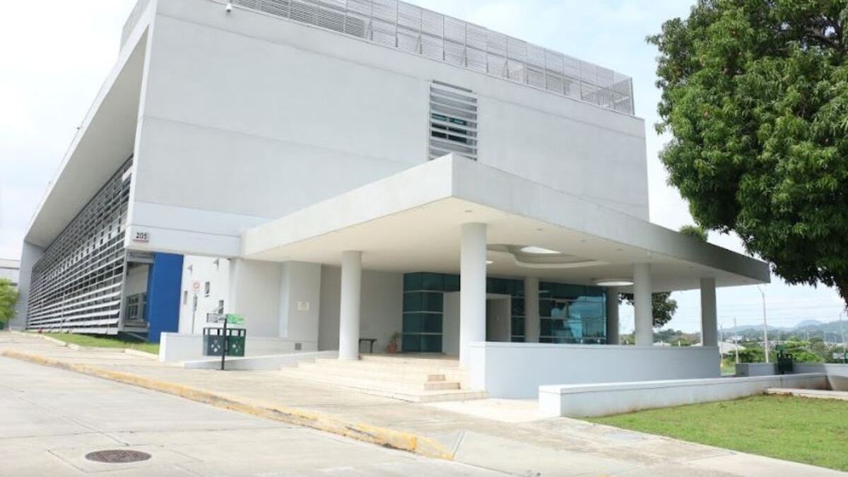
Panama’s Advanced Semiconductor Technology Center (C-TASC AIP) has launched a job call for a project coordinator who will oversee the design phase of its new building on the campus of the Technological University of Panama (UTP). Interested professionals have until October 31, 2026 to submit their applications.
What Happened
C-TASC AIP, the Advanced Semiconductor Technology Center, opened a hiring process to contract a project coordinator responsible for the design phase of its new facility. The building will be located on the campus of the Technological University of Panama (UTP), one of the country’s leading public universities focused on engineering and technology.
The position involves leading the coordination of the design stage of the construction project, a critical early phase that lays the groundwork for the future semiconductor technology facility. The application window remains open through the end of October 2026, giving qualified professionals with experience in projects time to prepare and submit their candidacies.
Background
C-TASC AIP is part of Panama’s emerging push into the semiconductor industry. In recent years, Panama has sought to position itself as a regional player in semiconductor research, development, and workforce training, leveraging its strategic location, logistics infrastructure, and academic institutions. The Technological University of Panama has served as a key partner in these efforts, hosting technology-focused initiatives and preparing engineers for advanced industries.
Semiconductors are the tiny chips that power everything from smartphones to cars to artificial intelligence systems, and countries worldwide are competing to secure a foothold in the global supply chain. For Panama, a nation whose economy has historically relied on the canal, banking, and logistics, developing a domestic semiconductor capability represents an effort to diversify into high-value technology sectors.
Building a physical home for the center on the UTP campus signals that the initiative is moving from planning toward concrete infrastructure, with the design phase being the first major step in constructing the facility.
What This Means for Panama
The job opening is a small but telling indicator that Panama’s semiconductor ambitions are advancing. Hiring a coordinator for the design phase means the project is entering an active stage, and the resulting construction could generate further opportunities for architects, engineers, and construction professionals in the coming years.
For professionals with project experience, the October 31, 2026 deadline offers a chance to join a strategically significant national initiative. The role also connects the selected candidate to the intersection of academia and industry, working within a university environment on a project tied to one of the world’s most important technology sectors.
Those interested should watch for application details through C-TASC AIP’s official channels and ensure their submissions are complete before the deadline. Beyond this single position, the progress of the building project will be worth monitoring as a measure of how quickly Panama’s semiconductor strategy translates into physical capacity and skilled jobs.
This story was originally reported by Telemetro.